HOT PRODUCTS
Show More
About Us
Founded in 2014, Bena was co-founded by several experienced engineers who have more than 10 years of optical design, process, production and test. We provide customization service for high precision (rms = 1/100λ, λ=632.8nm), large diameter plane mirror (>500mm) and aspherical lens, as well as professional spherical lens (such as Optical Domes with diameter 280mm), involving different materials including K9, Silicon, Sapphire, SiC, glass ceramics, fused silica, and other various optical glasses, and we can also deal with the nickel-phosphorus alloy surface on different substrates.
NEW PRODUCTS
Latest News
  • 08 2021.07
    On May 31, 2018, Hubei Zhijiang electronic information industrial park officially opened. On the same day, six electronic information enterprises were put into operation in the park, and seven projects were signed, with a total investment of 2.05 billion yuan. After the completion of the electronic information industrial park, it will become the largest optoelectronic core components production base in Central China, with an annual output value of 20 billion yuan. The electronic information industrial park is a green modern industrial park with new optoelectronic core components, mobile phones, tablet computers and other intelligent terminal manufacturing industries. It covers an area of 275 mu, with a planned total construction area of 230000 square meters. The whole park is constructed in two phases. The first phase has been completed. After the second phase is completed, it can accommodate nearly 100 enterprises and realize profits and taxes of 800 million yuan. 
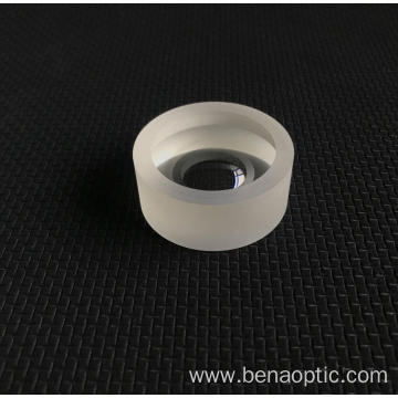
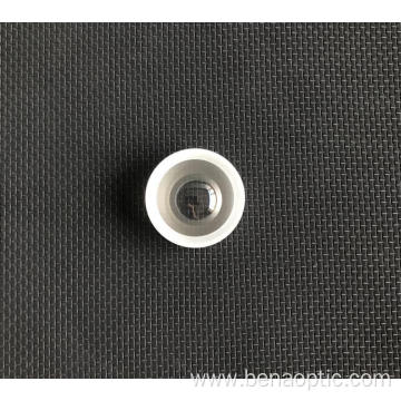
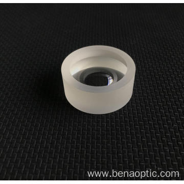
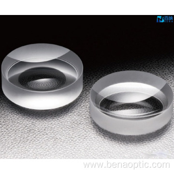
Electronic information enterprises have come to Zhijiang from Shenzhen and Dongguan, and all of them have realized intellectualization. For example, the cameras produced by Huaxin Optoelectronics in Shenzhen used to be 2-5 million pixels, and now the cameras produced in Zhijiang are 8-13 million pixels; It used to be a single camera, but now it is a dual camera, a three camera, and a panoramic 360 degree camera; In the past, six people managed one device in Shenzhen, but now one person manages six devices in Zhijiang. At present, the park has initially formed an industrial closed-loop from mobile phone lens, light filter, motor, camera module, touch screen, LCD module to the whole machine terminal. Zhijiang electronic information industry has created two "Zhijiang speed" from scratch. First, the electronic information industrial park will be built in half a year; The first is to carry out the whole process of examination and approval procedures, and handle all the licenses for the ent
    READ MORE
  • 08 2021.07
    On April 30, 2020, the project of semiconductor photoelectric industrial chain Park invested and established by Suzhou Nachuan Investment Management Co., Ltd. was signed and settled in Nantong high tech Zone. Chenyonghong, Secretary of Nantong hi tech Zone Committee and Secretary of the Party Working Committee of Nantong high tech Zone attended the signing ceremony. The project is supported by capital, based on the development experience of nano industry in Suzhou Industrial Park, led by "semiconductor photoelectric industry", assisted by intelligent manufacturing, supplemented by other strategic emerging industries, and introduced scientific research institutes and international innovation centers, established a set of Industrial Fund for science and Technology Park, and built a "scientific research, achievement transformation and industrialization" in one Pan semiconductor photoelectric industry cluster with 10 billion production value. It is reported that the total investment of the project is 3 billion yuan, and it is planned to attract about 40 high-tech enterprises, and strive to introduce and independently cultivate 2-3 listed enterprises, and the expected output value after reaching the production can exceed 5 billion yuan. The project is led by "semiconductor photoelectric industry", assisted by intelligent manufacturing, supplemented by other strategic emerging industries, and introduced scientific research institutes and international innovation centers, established supporting industrial fund of science and Technology Park, and built a pan semiconductor photoelectric industry cluster with "scientific research, achievement transformation and industrialization" and 10 billion level output value. The total investment of the project is 3 billion yuan, and it is planned to attract about 40 high-tech enterprises, strive to introduce and independently cultivate 2-3 listed enterprises, and the expected output value after reaching the post natal peri
    READ MORE
Related Products List

Home

Product

Phone

About Us

Inquiry

We will contact you immediately

Fill in more information so that we can get in touch with you faster

Privacy statement: Your privacy is very important to Us. Our company promises not to disclose your personal information to any external company with out your explicit permission.

Send